
Let us discuss clock gating in simplest terms.
Definition :
Technique to switch off the clock when not in use. It reduces the switching activity and hence, saves dynamic power, without affecting the design functionality.
Simplest Clock Gating
Naming:
‘en’: Enable signal.
‘clk’: The non-gated original clock
‘g_clk’: Gated clock (off when not in use)
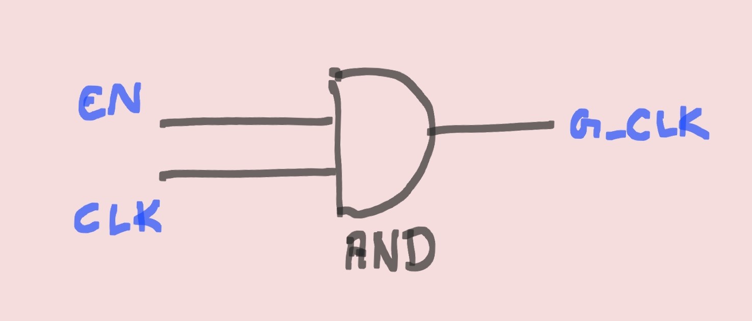
Working:
When ‘en’ is 1: Clock goes to the next flop
When ‘en’ is 0: Clock to the next flop is blocked by AND gate.
Pros and Cons:
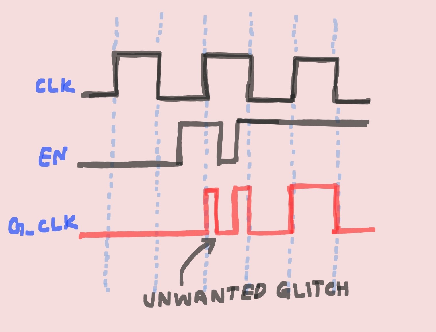
++ Simple, easy to code, consumes less area
— Can cause glitches in the gated clock. (If the change in ‘en’ occurs when clk is ‘1’ as given, it causes glitches in the gated clock.)
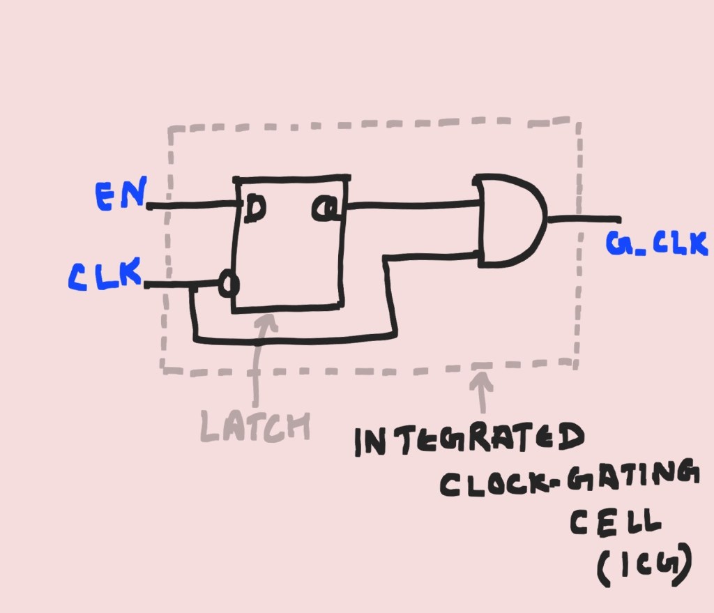
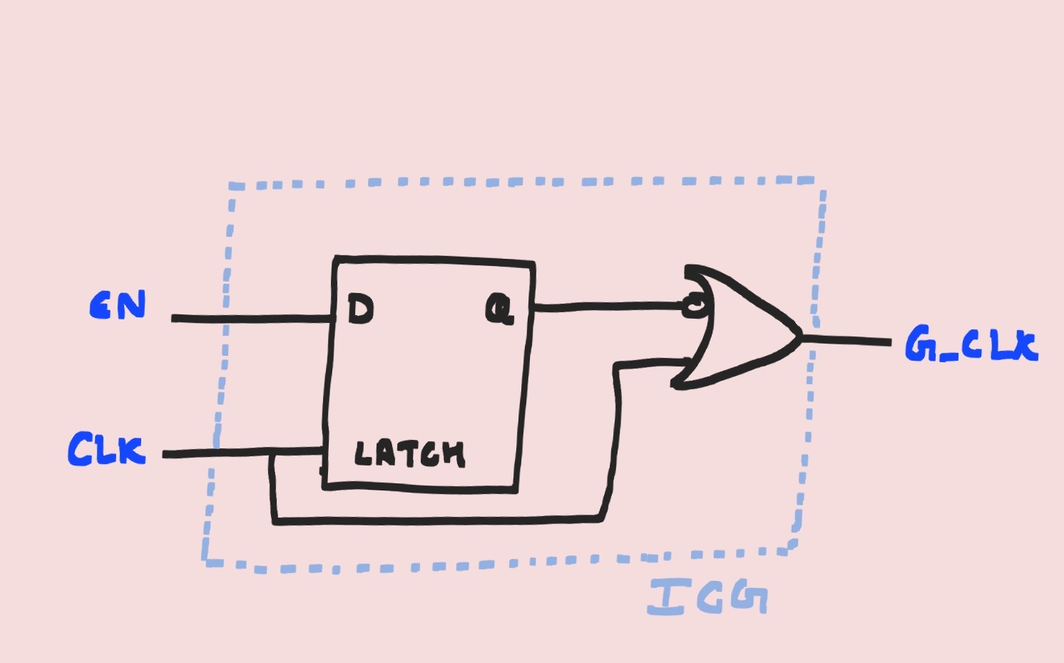
Latch Based Clock Gating
Use a latch (level-sensitive) to create a glitch-free clock gating cell.
Naming:
‘en’: Enable signal.
‘clk’: The non-gated original clock
‘g_clk’: Gated clock (off when not in use)
‘latch’: D-latch (negatively triggered i.e. allows the input to pass when clk is ‘0’ )
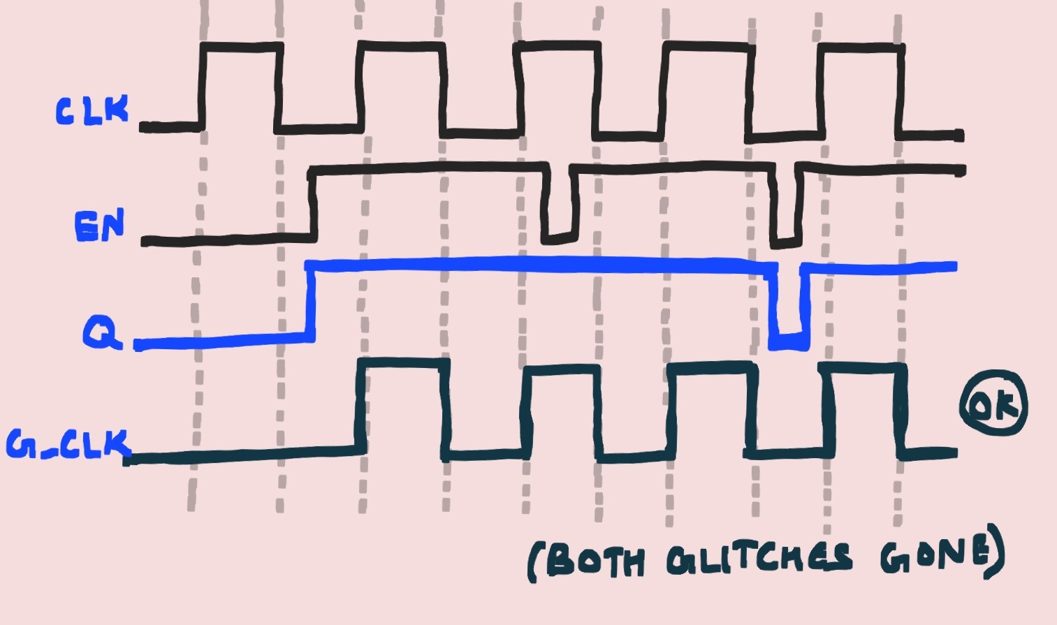
Glitch Free Behavior
This is a modification of simplest clock gating, by introducing a negative latch as shown. When clock is ‘1’, the latch doesn’t allow the glitch in ‘en’ signal to pass to the latch output ‘Q’. It holds the previous value when clk signal was ‘0’, hence eliminating the glitch in gated clock.
Additional Points
- The clock gating insertion is mostly done by the tools nowadays, while performing the synthesis operation. The above circuits discussed are referred as ICGs (Integrated Clock Gating Circuits), which are added by the tool based on the commands given by the engineers.
- The ‘en’ signal used in the design can come from software, or can be a hardware generated signal. The simplest example of hardware derived enable is: ‘en’ is the XOR output of the ‘D’ and ‘Q’ of the next gated flop. This way, ‘en’ is 1 only when the value of ‘D’ and ‘Q’ differs i.e. flip-flop value needs to be updated.
- We discussed a negative latch and AND based circuit above. Glitch free gated clock can also be derived by a positive latch and an OR gate circuit. The diagram is as follows:
Get new content delivered directly to your inbox.

Leave a reply to Anonymous Cancel reply